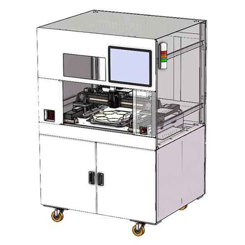
This device measures the thickness of wafers and display panels after partial processes such as wafer slicing, grinding, thinning, and slicing. Can synchronously test the TTVBOWWRAP/SORI and other parameter errors of the material itself.
|
Project |
Performance index |
|
Use ceramic disc size |
φ260/268/305/360mm, Automated loading and unloading of robotic arms |
|
Equipment measurement resolution |
0.005um |
|
Measurement repeatability |
≤0.5um |
|
Measurement accuracy |
≤ 1um (measurement comparison accuracy is affected by ceramic disc and wax layer) |
|
Measuring range |
0-1000um |
|
Number of measurement points |
1. 3, 5, 9... N (number of points can be set) |
|
Measurement efficiency |
Fastest 18sec/p, 5-point sampling |
|
Measure bandwidth |
Max 10000Point/sec |
|
Measure material |
Transparent, non transparent, smooth, rough samples such as GaN, GaAs, Si, SiN, Sic, etc |
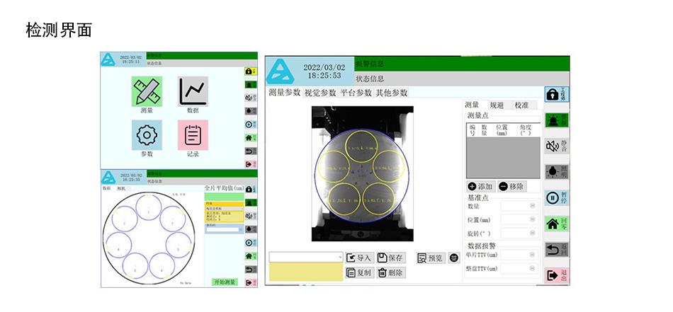
This device measures the thickness of wafers and display panels after partial processes such as wafer slicing, grinding, thinning, and slicing. Can synchronously test the TTVBOWWRAP/SORI and other parameter errors of the material itself.
View More
The wafer scratch AOI inspection machine is mainly used for detecting obvious scratch defects such as missed scratches, defocusing, uncut, and bicrystals on the core grains on the Disco ring after wafer splitting machine processing. Through Machine Vision defect detection, the presence or absence of the above defects can be detected to distinguish between good and defective products, reduce manual labor, and improve detection efficiency.
View More
Solid state wire bonding AOI inspection machine, also known as wire bonding AOI inspection machine, is mainly used for efficient AOI inspection of defects after die bonding and wire bonding in the semiconductor packaging and testing field. It has the characteristics of high speed, high precision, and high inspection coverage. Optical system modules and core detection algorithms with completely independent intellectual property rights, as well as AI deep learning algorithms, are suitable for detecting various defects on grain surfaces, solder joints, solder wires, and frame surfaces that occur during the solidification and wire bonding processes.
View More
The shape and distribution of dislocation defects in semiconductor wafer preparation have a significant impact on the performance of electronic components. Due to differences in doping materials and preparation processes, the distribution of dislocations also varies. This device is used to inspect the morphology and distribution of wafer dislocations, providing data support for wafer material research and improving preparation processes. Suitable for 2-inch, 3-inch, 4-inch, and 6-inch gallium arsenide substrates.
View More Address:Unit 204, No. 30 Guanri Road, Phase II Software Park, Xiamen City
Factory Address:1st Floor,Great Wall Business Building,76-78 Huli Avenue,Xiamen City
Address:Unit 204, No. 30 Guanri Road, Phase II Software Park, Xiamen City
Factory Address:1st Floor,Great Wall Business Building,76-78 Huli Avenue,Xiamen City
 Consultation Hotline:86-0592-3799658、86-137 9991 1773(Switchboard)
 Email : AOI@otek.com.cn